Что такое корпуса QFP, LQFP и TQFP. Каковы их основные характеристики и применения. Чем отличаются разновидности этих корпусов. Как выбрать оптимальный тип корпуса для конкретной задачи. Какие преимущества дает использование этих корпусов в электронных устройствах.
Что представляют собой корпуса QFP, LQFP и TQFP?
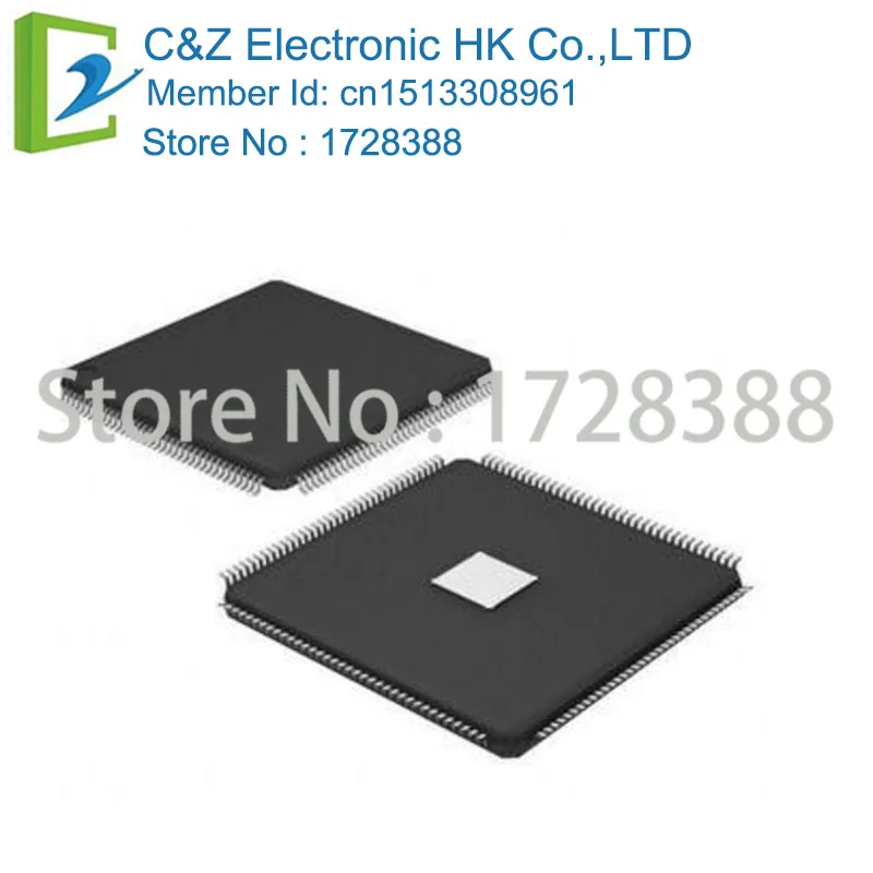
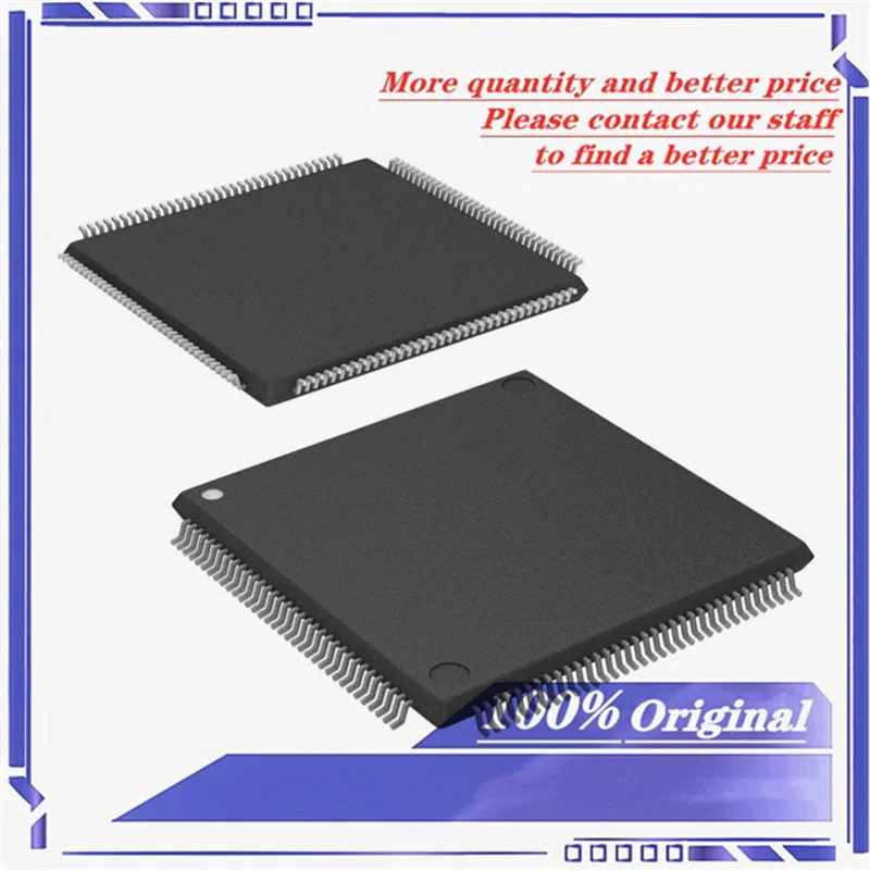
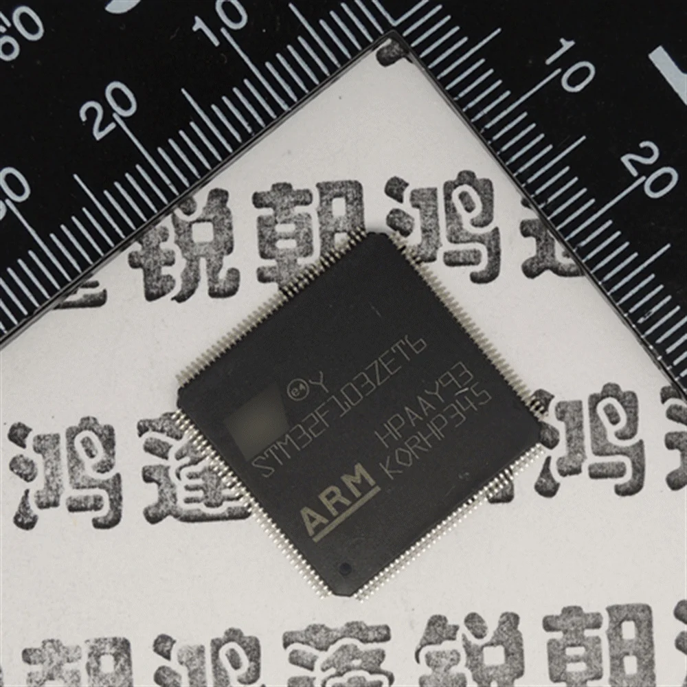
Корпуса QFP (Quad Flat Package), LQFP (Low-profile Quad Flat Package) и TQFP (Thin Quad Flat Package) являются популярными типами корпусов для интегральных микросхем. Они относятся к семейству планарных корпусов с четырехсторонним расположением выводов.
Основные характеристики этих корпусов:
- Квадратная или прямоугольная форма
- Выводы расположены по всем четырем сторонам корпуса
- Выводы имеют форму «чайки» (gull-wing)
- Малая толщина корпуса
- Высокая плотность монтажа на печатной плате
Чем отличаются разновидности этих корпусов? QFP имеет стандартную толщину, LQFP — уменьшенную высоту профиля, а TQFP — сверхтонкое исполнение. Это позволяет подобрать оптимальный вариант для различных применений.
Ключевые особенности и преимущества корпусов семейства QFP
Корпуса семейства QFP обладают рядом важных преимуществ:
- Высокая плотность монтажа — до 208 выводов при малых габаритах
- Хороший теплоотвод за счет большой площади корпуса
- Удобство автоматизированного монтажа
- Визуальный контроль качества пайки
- Широкий выбор типоразмеров
- Доступная цена по сравнению с BGA
Какие задачи решают эти особенности? Они позволяют создавать компактные устройства с высокой функциональностью, упрощают производственный процесс и снижают себестоимость продукции.
Разновидности корпусов QFP и их применение
Семейство QFP включает множество разновидностей, различающихся количеством выводов и шагом между ними:
- QFP28-208 — от 28 до 208 выводов
- TQFP64-168 — сверхтонкие корпуса с 64-168 выводами
- LQFP32-144 — низкопрофильные корпуса с 32-144 выводами
Где применяются различные типы QFP-корпусов? QFP с большим числом выводов используются для мощных процессоров и ПЛИС. TQFP популярны в портативной электронике. LQFP часто применяются в автомобильной электронике и промышленной автоматике.
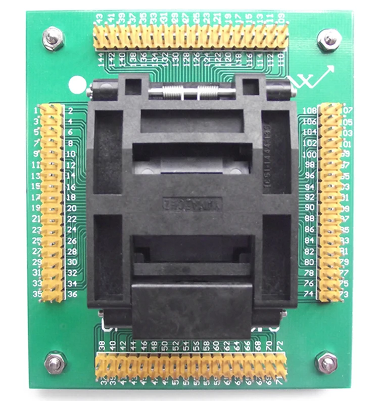
LQFP144 — особенности и применение
LQFP144 — один из наиболее распространенных представителей семейства. Его ключевые характеристики:
- 144 вывода
- Шаг выводов 0.5 мм
- Размеры корпуса 20×20 мм
- Высота профиля 1.4 мм
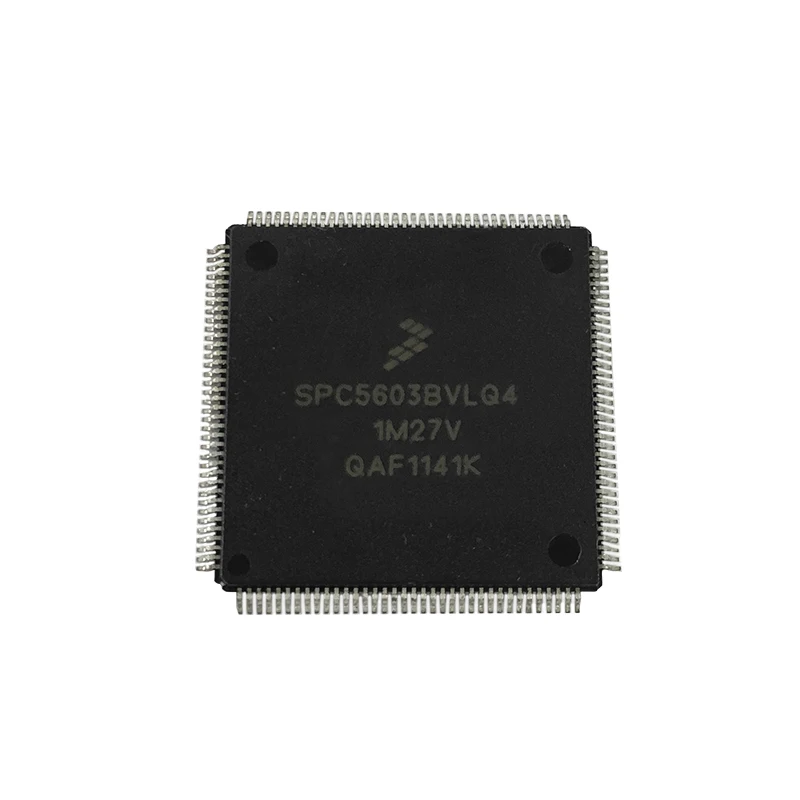
Для каких микросхем используется LQFP144? Этот корпус часто применяется для мощных микроконтроллеров, таких как серия STM32F4 от STMicroelectronics или LPC1850 от NXP Semiconductors. Он обеспечивает оптимальный баланс между количеством выводов, габаритами и теплоотводом.
Особенности монтажа корпусов QFP, LQFP и TQFP
Монтаж корпусов семейства QFP имеет свои нюансы:
- Требуется точное позиционирование на плате
- Необходимо контролировать количество припоя
- Важно избегать образования перемычек между выводами
- Рекомендуется использование паяльной пасты и оплавление в печи
Как обеспечить качественный монтаж QFP-корпусов? Ключевые факторы — это правильно разработанная топология печатной платы, использование качественного оборудования и соблюдение температурного профиля пайки. При ручном монтаже важно применять флюс и работать с максимальной аккуратностью.
Сравнение QFP с другими типами корпусов
Как QFP соотносятся с другими популярными типами корпусов?
- По сравнению с DIP — выше плотность монтажа, меньше занимаемая площадь
- В сравнении с BGA — проще монтаж и визуальный контроль, но меньше выводов
- Относительно LGA — лучше теплоотвод, но больше габариты
Какой тип корпуса выбрать для конкретной задачи? Это зависит от требований к устройству. QFP оптимальны, когда нужен баланс между количеством выводов, простотой монтажа и стоимостью. Для сверхкомпактных устройств лучше подойдут BGA, а для простых схем — DIP или SOP.
Тенденции развития корпусов для микросхем
Какие тенденции наблюдаются в развитии корпусов микросхем?
- Уменьшение шага между выводами
- Снижение высоты профиля
- Улучшение теплоотвода
- Повышение надежности и устойчивости к внешним воздействиям
Как это влияет на применение QFP-корпусов? С одной стороны, они продолжают совершенствоваться и находят новые области применения. С другой — в некоторых сферах их вытесняют более компактные решения типа BGA и CSP. Однако QFP сохраняют свои позиции там, где важна простота монтажа и ремонтопригодность.
Выбор оптимального корпуса для конкретной задачи
При выборе корпуса микросхемы необходимо учитывать множество факторов:
- Требуемое количество выводов
- Ограничения по габаритам устройства
- Условия эксплуатации (температура, вибрации и т.д.)
- Технологические возможности производства
- Стоимость монтажа и контроля качества
Как правильно выбрать корпус микросхемы? Оптимальный подход — это комплексный анализ всех требований к устройству и возможностей производства. Важно найти баланс между техническими характеристиками, технологичностью и стоимостью.
Особенности проектирования печатных плат для QFP-корпусов
При разработке печатных плат для микросхем в QFP-корпусах следует учитывать ряд важных моментов:
- Правильный расчет посадочного места
- Оптимальная трассировка выводов
- Обеспечение теплоотвода
- Учет паразитных емкостей и индуктивностей
- Размещение декупляжных конденсаторов
Как обеспечить качественную разводку платы под QFP? Ключевые рекомендации включают использование специализированного ПО для проектирования, соблюдение правил высокочастотной разводки, применение полигонов для земли и питания. Важно также учитывать требования по электромагнитной совместимости.

Контроль качества монтажа QFP-корпусов
Для обеспечения надежности устройств критически важен контроль качества монтажа QFP-корпусов. Основные методы контроля включают:
- Визуальный осмотр
- Рентгеновский контроль
- Оптическую инспекцию
- Электрическое тестирование
- Термографический анализ
Как выявить дефекты монтажа QFP-микросхем? Визуальный осмотр позволяет обнаружить очевидные проблемы — перемычки, отсутствие пайки. Рентген помогает выявить скрытые дефекты — пустоты в паяных соединениях. Электрическое тестирование и термография позволяют найти проблемные участки в работающем устройстве.
Перспективы развития технологии QFP
- Уменьшение шага выводов до 0.3 мм и менее
- Улучшение теплоотвода за счет применения новых материалов
- Повышение устойчивости к механическим воздействиям
- Оптимизация формы выводов для улучшения монтажа
- Разработка вариантов с экранированием для высокочастотных применений
Какое будущее ждет корпуса QFP? Они, вероятно, сохранят свои позиции в сегменте средней сложности устройств, где важен баланс между функциональностью, простотой монтажа и стоимостью. В то же время, в области сверхкомпактных устройств их будут вытеснять BGA и CSP, а для простых применений останутся актуальны SOP и SOIC.
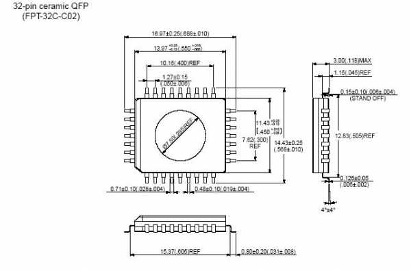
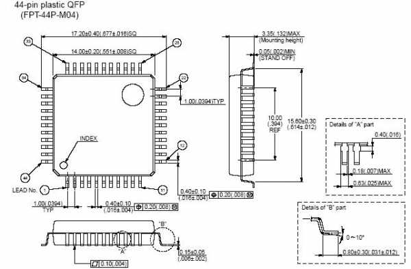
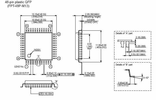
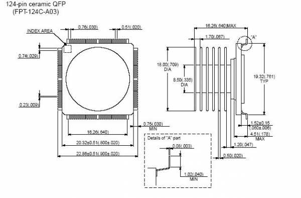
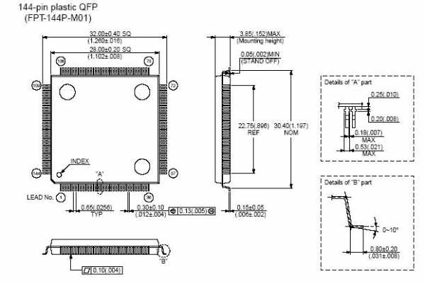
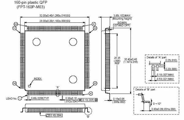
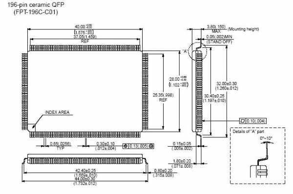
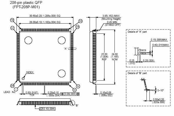
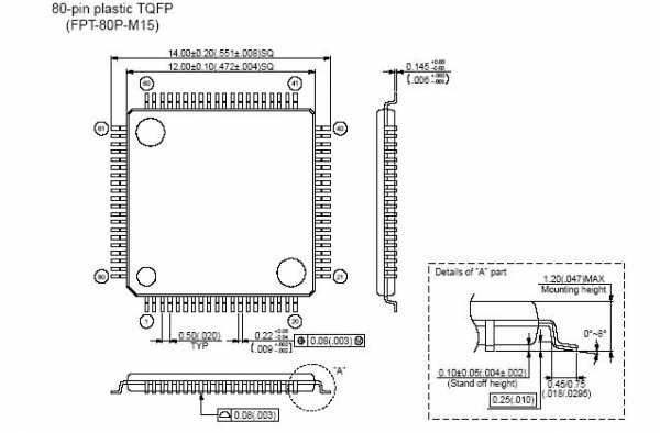
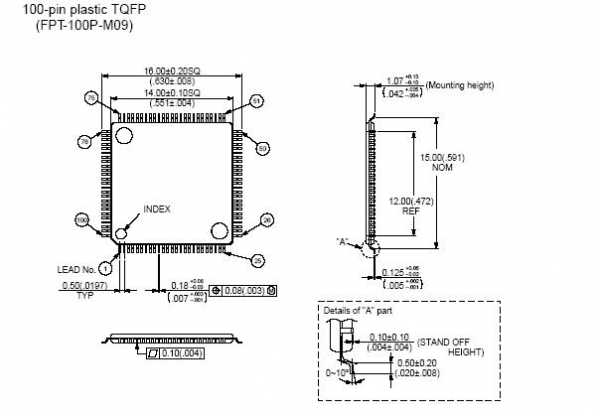
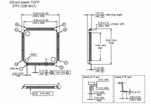
Корпуса QFP, LQFP, TQFP. Чертежи корпусов импортных микросхем.
QFP28

QFP32
QFP44
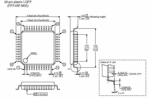
QFP48
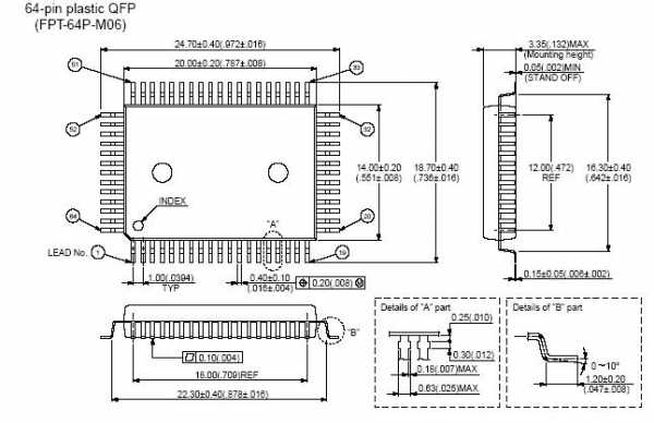
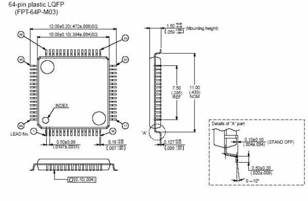
QFP64
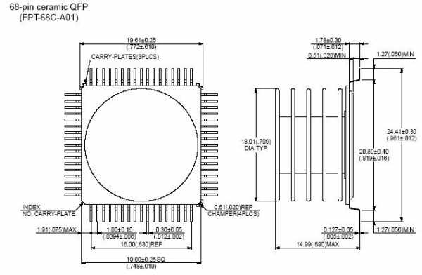
QFP68
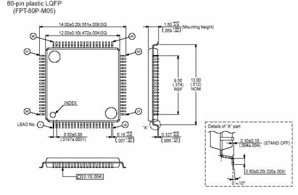
QFP80

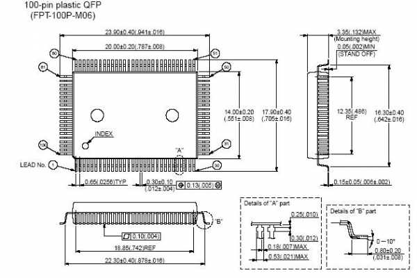
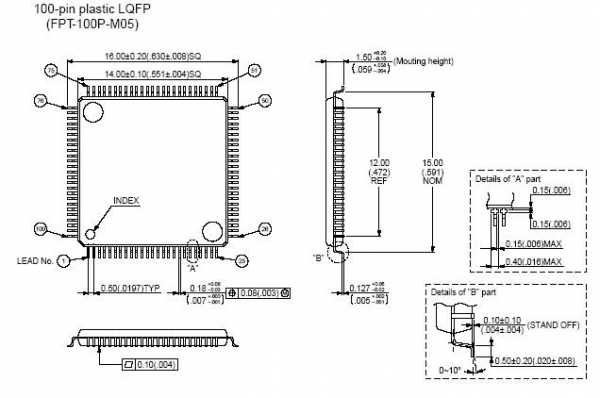
QFP100
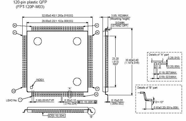
QFP120
QFP124
QFP144
QFP160
QFP164

QFP176

QFP196
QFP208
TQFP64

TQFP80
TQFP100
TQFP120
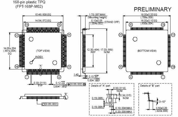
TQFP168
LQFP32

LQFP48
LQFP64
LQFP80
LQFP100
LQFP120

LQFP144
 Все типы корпусов импортных микросхем
Печатать
www.chipdip.ru
NXP Semiconductors. LQFP144 Даташит, LQFP144 PDF, даташитов
General description
The LPC1850/30/20/10 are ARM Cortex-M3 based microcontrollers for embedded applications. The ARM Cortex-M3 is a next generation core that offers system enhancements such as low power consumption, enhanced debug features, and a high level of support block integration.
The LPC1850/30/20/10 operate at CPU frequencies of up to 180 MHz. The ARM Cortex-M3 CPU incorporates a 3-stage pipeline and uses a Harvard architecture with separate local instruction and data buses as well as a third bus for peripherals. The ARM Cortex-M3 CPU also includes an internal prefetch unit that supports speculative branching.
The LPC1850/30/20/10 include up to 200 kB of on-chip SRAM, a quad SPI Flash Interface (SPIFI), a State Configurable Timer (SCT) subsystem, two High-speed USB controllers, Ethernet, LCD, an external memory controller, and multiple digital and analog peripherals.
Features and benefits
■ Processor core
◆ ARM Cortex-M3 processor, running at frequencies of up to 180 MHz.
◆ ARM Cortex-M3 built-in Memory Protection Unit (MPU) supporting eight regions.
◆ ARM Cortex-M3 built-in Nested Vectored Interrupt Controller (NVIC).
◆ Non-maskable Interrupt (NMI) input.
◆ JTAG and Serial Wire Debug, serial trace, eight breakpoints, and four watch points.
◆ Enhanced Trace Module (ETM) and Enhanced Trace Buffer (ETB) support.
◆ System tick timer.
■ On-chip memory
◆ 200 kB SRAM for code and data use.
◆ Multiple SRAM blocks with separate bus access.
◆ 64 kB ROM containing boot code and on-chip software drivers.
◆ 32-bit One-Time Programmable (OTP) memory for general-purpose use.
■ Clock generation unit
◆ Crystal oscillator with an operating range of 1 MHz to 25 MHz.
◆ 12 MHz internal RC oscillator trimmed to 1 % accuracy over temperature and
voltage.
◆ Ultra-low power RTC crystal oscillator.
◆ Three PLLs allow CPU operation up to the maximum CPU rate without the need for
a high-frequency crystal. The second PLL is dedicated to the High-speed USB, the
third PLL can be used as audio PLL.
◆ Clock output.
■ Configurable digital peripherals:
◆ State Configurable Timer (SCT) subsystem on AHB.
◆ Global Input Multiplexer Array (GIMA) allows to cross-connect multiple inputs and
outputs to event driven peripherals like timers, SCT, and ADC0/1.
■ Serial interfaces:
◆ Quad SPI Flash Interface (SPIFI) with 1-, 2-, or 4-bit data at rates of up to
52 MB per second.
◆ 10/100T Ethernet MAC with RMII and MII interfaces and DMA support for high
throughput at low CPU load. Support for IEEE 1588 time stamping/advanced time
stamping (IEEE 1588-2008 v2).
◆ One High-speed USB 2.0 Host/Device/OTG interface with DMA support and
on-chip high-speed PHY (USB0).
◆ One High-speed USB 2.0 Host/Device interface with DMA support, on-chip
full-speed PHY and ULPI interface to an external high-speed PHY (USB1).
◆ USB interface electrical test software included in ROM USB stack.
◆ Four 550 UARTs with DMA support: one UART with full modem interface; one
UART with IrDA interface; three USARTs support UART synchronous mode and a
smart card interface conforming to ISO7816 specification.
◆ Up to two C_CAN 2.0B controllers with one channel each. Use of C_CAN controller
excludes operation of all other peripherals connected to the same bus bridge See
Figure 1 and Ref. 1.
◆ Two SSP controllers with FIFO and multi-protocol support. Both SSPs with DMA
support.
◆ One Fast-mode Plus I2C-bus interface with monitor mode and with open-drain I/O
pins conforming to the full I2C-bus specification. Supports data rates of up to
1 Mbit/s.
◆ One standard I2C-bus interface with monitor mode and standard I/O pins.
◆ Two I2S interfaces with DMA support, each with one input and one output. (Continue …)
ru.datasheetbank.com
Корпуса микросхем типа QFP, TQFP и LQFP | Электронные компоненты
Корпуса микросхем QFP, TQFP, LQFP\Step AP214\Корпус LQFP-100 (0.50 мм).STEP
Корпуса микросхем QFP, TQFP, LQFP\Step AP214\Корпус LQFP-120 (0.40 мм).STEPКорпуса микросхем QFP, TQFP, LQFP\Step AP214\Корпус LQFP-144 (0.50 мм).STEP
Корпуса микросхем QFP, TQFP, LQFP\Step AP214\Корпус LQFP-32 (0.80 мм).STEP
Корпуса микросхем QFP, TQFP, LQFP\Step AP214\Корпус LQFP-48 (0.50 мм).STEP
Корпуса микросхем QFP, TQFP, LQFP\Step AP214\Корпус LQFP-64 (0.50 мм).STEP
Корпуса микросхем QFP, TQFP, LQFP\Step AP214\Корпус LQFP-80 (0.50 мм).STEP
Корпуса микросхем QFP, TQFP, LQFP\Step AP214\Корпус QFP-100 (0.65 мм).STEP
Корпуса микросхем QFP, TQFP, LQFP\Step AP214\Корпус QFP-120 (0.80 мм).STEP
Корпуса микросхем QFP, TQFP, LQFP\Step AP214\Корпус QFP-144 (0.65 мм).STEP
Корпуса микросхем QFP, TQFP, LQFP\Step AP214\Корпус QFP-160 (0.65 мм).STEP
Корпуса микросхем QFP, TQFP, LQFP\Step AP214\Корпус QFP-176 (0.50 мм).STEP
Корпуса микросхем QFP, TQFP, LQFP\Step AP214\Корпус QFP-196 (0.65 мм).STEP
Корпуса микросхем QFP, TQFP, LQFP\Step AP214\Корпус QFP-208 (0.50 мм).STEP
Корпуса микросхем QFP, TQFP, LQFP\Step AP214\Корпус QFP-44 (1.00 мм).STEP
Корпуса микросхем QFP, TQFP, LQFP\Step AP214\Корпус QFP-48 (0.80 мм).STEP
Корпуса микросхем QFP, TQFP, LQFP\Step AP214\Корпус QFP-64 (1.00 мм).STEP
Корпуса микросхем QFP, TQFP, LQFP\Step AP214\Корпус QFP-80 (0.80 мм).STEP
Корпуса микросхем QFP, TQFP, LQFP\Step AP214\Корпус TQFP-100 (0.50 мм).STEP
Корпуса микросхем QFP, TQFP, LQFP\Step AP214\Корпус TQFP-120 (0.40 мм).STEP
Корпуса микросхем QFP, TQFP, LQFP\Step AP214\Корпус TQFP-168 (0.30 мм).STEP
Корпуса микросхем QFP, TQFP, LQFP\Step AP214\Корпус TQFP-64 (0.50 мм).STEP
Корпуса микросхем QFP, TQFP, LQFP\Step AP214\Корпус TQFP-80 (0.50 мм).STEP
Корпуса микросхем QFP, TQFP, LQFP\Корпус QFP, LQFP, TQFP.SLDPRT
Корпуса микросхем QFP, TQFP, LQFP\Step AP214
Корпуса микросхем QFP, TQFP, LQFP
vmasshtabe.ru